![]()
![]()
![]()
![]()
![]()
![]()
![]()
![]()
![]()
Substrate Material:
Standard:
0.004"(0.10mm) or 0.005"(0.125mm) Polyester (PET), translucent and white
Available:
0.003"(0.08mm) through 0.010"(0.25mm) Polyester, as well as other substrates for custom applications
Sheet Sizes:
The print area maximum is a 24" X 36" sheet.
The sheet size for component placement is 18" X 24" with a placement area of 18" X 22"Conductive Inks (typical values):
PF012
Ag/PET
20m W/sq./0.001"(0.025mm)
PF014
Ag/PET
15m W/sq./0.001"(0.025mm),(hardness >2H)
PF308
C/PET
30 W/sq./0.001"(0.025mm)
Dielectric Materials:
PF114
Flexible, moisture resistant, UV cure dielectric suitable for use as a printed spacer, covercoat, and as insulation between conductive layers.
Circuit Density:
Spacing:
Standard is 0.010"(.25mm) lines and spaces or greater. Finer lines and spaces can be evaluated on a by application basis.
Conductive Layers:
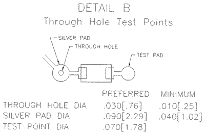
Up to 6 layers (3 per side of the substrate), assuming 1 layer per side is a shield or ground. Printed througholes and printed crossovers are utilized in circuit design.
To view througholes test point, see Detail "B"
Print Registration:
+/-0.006" (0.15mm) print to print (each side)
+/-0.010" (0.25mm) top surface to bottom surfaceDie Cut to Print (referenced from one edge):
Hard Tool:
+/-0.010"(0.25mm)
Steel rule die:
+/-0.015"(0.375mm)
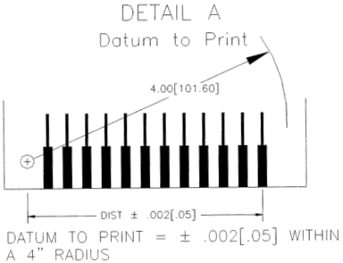
Optically registered punch (datum) to print registration of +/-0.004"(0.10mm) within a 4"(100mm) radius from datum. See Detail "A"
Flexibility:
Trace / conductor may be flexed around a .125"(3.125mm) minimum radius under both compression and tension. Circuits may be flexed in the component area around a 4" (100mm) radius under both compression and tension.
Trace Resistance of PF014 ink:
A 2.5 W/inch (25mm) resistance is typical for a 0.020" (.50mm) wide trace at nominal ink thickness of 0.0003" (0.008mm) microns. Resistance change as a function of line width is
inversely proportional when ink thickness is constant (i.e.: resistance of a 0.040" (1mm) wide trace at 0.0003" (0.008mm) thickness = 1.25 W/inch(25mm)
The formula to calculate linear resistance is:
ink resistance X length/width X 1/thickness = W
SMD Junction Resistance:
<30m W typical per junction
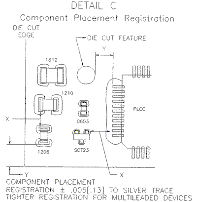
Components:
Chip Resistors and capacitors (0603 minimum package size)
SMT LED's
QFP, SOIC, and PLCC packages (>/-.020" (0.50mm)pitch)
Bare die per application
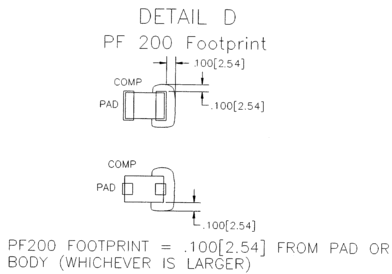
To view component registration, see Detail "C"Mechanical Strength of Poly-Solder® & PF200 UV Curable Strain Relief Material:
Two leaded components (LED's, resistors and capacitors):
Typical shear strength 5lb.(2.25kg) minimum after attachment:
After PF200 is applied and cured (for mechanical strain relief), value typically doubles to 10lb.(4.5kg)
Multi-leaded components:
Varies, however typical shear of .75lb/lead (.35kg) after attachment and normally >1lb/lead (.45kg) after PF200 applied and cured.
To view PF200 footprint see Detail "D"
Environmental Specifications:
Operating Temperature:
-40°C to +85°C Please consult Sales and Engineering for applicability outside of these values.
Humidity:
5% to 90% RH non-condensing
Storage / Shipping:
-40°C to +85°C
5% to 90% RH non-condensingShock:
Thermal: -40°C to +85°C, 25 cycles
Mechanical: 30G, 11msec., half sine wave
Vibration: 5.35 G rms, 50-2000 HzFlammability w/ PTF printed circuits:
Polyester UL 94 HB
Polyimide UL 94 V1
Polyetherimide UL 94 V1Connectors:
10 insertions and removals - specify PTF circuit version.
AMP Triomate 520314
0.100" (2.5mm) pitch
ELCO 6208 (PTF special)
0.040" (1mm) pitch
Molex 52610
0.040" (1mm) pitch
NOTE: Above connectors are suggestions only, please discuss this with Poly-Flex Sales and Engineering.
Data Transfer - CAD Files:
Process
Preferred
Alternatives
PCB Design
PADS, Power PCB
Gerber (ASCII / HPGL)
Mechanical Data
AutoCAD
DXF, Format (hardcopy)
Bill of Material
Max MRP
Hardcopy
Assembly Drawings
AutoCAD
Hardcopy
Schematics
PADS Logic
Net list, hardcopy